VIBE2
VIBE2 Support Information
Contents
[hide]Overview
VIBE2 is second generation IoT hardware platform by Yantrr, which provides a unique combination of industrial sensor interfaces (Ethernet, SPI, I2C, RS232, CAN, GPIO, PWM, ADC), worldwide 3G/HSPA+ connectivity (US carriers certified), optional local area WiFi & Bluetooth Low Energy (BT4.1) networking and a low power ARM processor for both industrial machine-to-machine (M2M) and home IoT applications. In an approximately 2x credit card size board, VIBE2 modularl design integrates wireless LAN/WAN connectivity with a powerful CPU system based on TI's popular AM335x Sitara ARM Cortex-A8 processors (600MHz to 1GHz options) complemented by 512MB (standard) DDR3 memory and abundant 4GB eMMC FLASH memory.
Key Features
Application Processor (BeagleBone compatible):
- TI Sitara™ ARM® Cortex®-A8 AM335x , up to 1GHz, 2000MIPS with 512 MB RAM, 4GB eMMC FLASH
- Supports UART/I2C/SPI/SDIO/CAN interfaces for sensor & machine data
- Standard BeagleBone headers for existing cape compatibility (See cape compatibility matrix)
- MicroSD storage
- Optional HDMI video
- 10/100M Ethernet
- Ships with Debian ARMHF OS
Enhanced for M2M:
- Multi-port USB hub with 4x USB-A host connectors for connecting additional USB devices
- High precision battery backed RTC
- Optional battery circuit for standby purposes with reverse voltage protection, battery charging and thermistor cutout
Connectivity & IoT Enablement:
- Wireless modem options
- PTCRB certified GSM/WCDMA HSPA+ multi-band modem (Up to 21/5.76 Mbps DL/UL data rates), optional integrated GPS.
- Verizon certified 1xRTT & EV-DO Rev. A (3.1/1.8 Mbps DL/UL data rates), optional integrated GPS.
- Global bands HSPA+/3G/2G modem (Up to 21/5.76 Mbps DL/UL data rates).
- CE certified LTE FDD [3,7,20] (50/100 Mbps DL/UL data rates), optional integrated GPS.
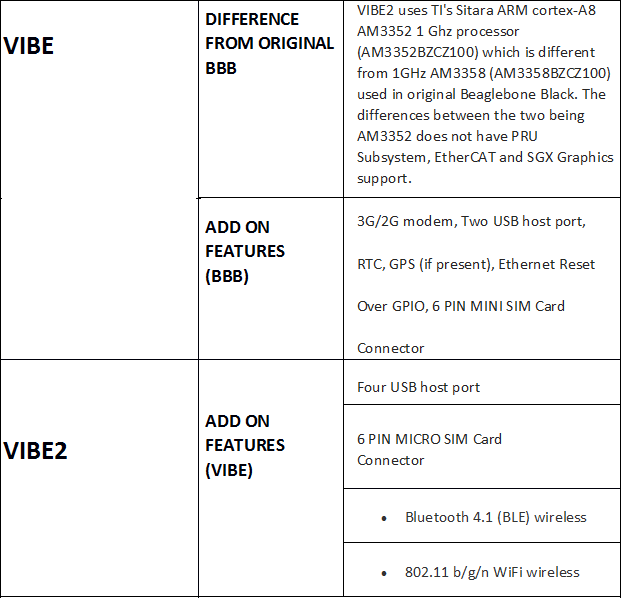
- Optional Bluetooth 4.1 (BLE) wireless
- Optional 802.11 b/g/n WiFi wireless
- Push-Push Mini SIM socket
- u.FL connectors for attaching modem antennas
- Optional Dedicated GPS+Timing Module with 1PPS output on a u.FL connector or GPIO
Hardware Configuration
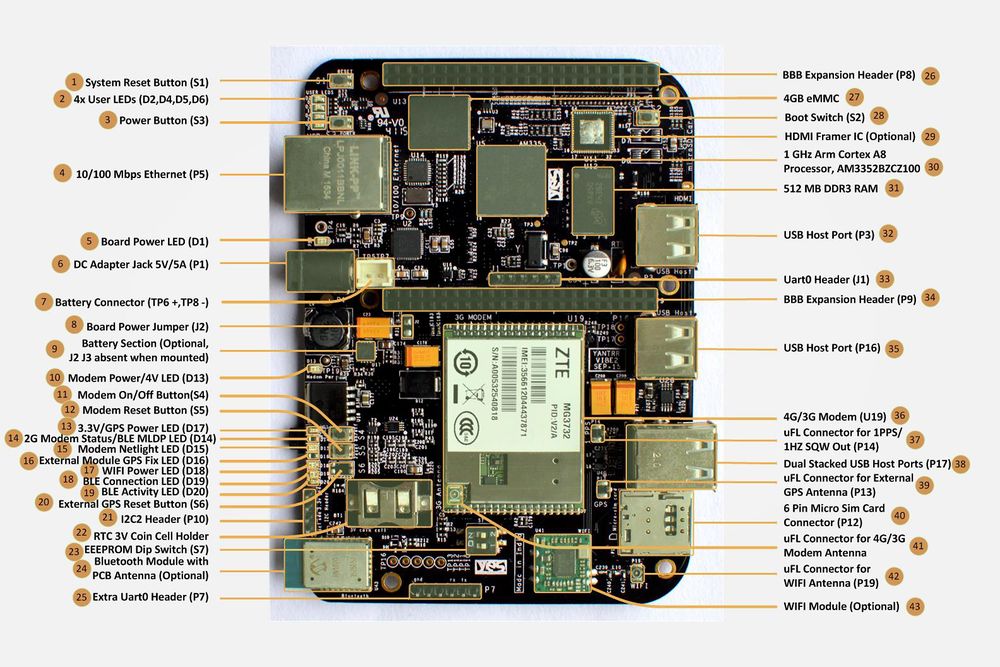
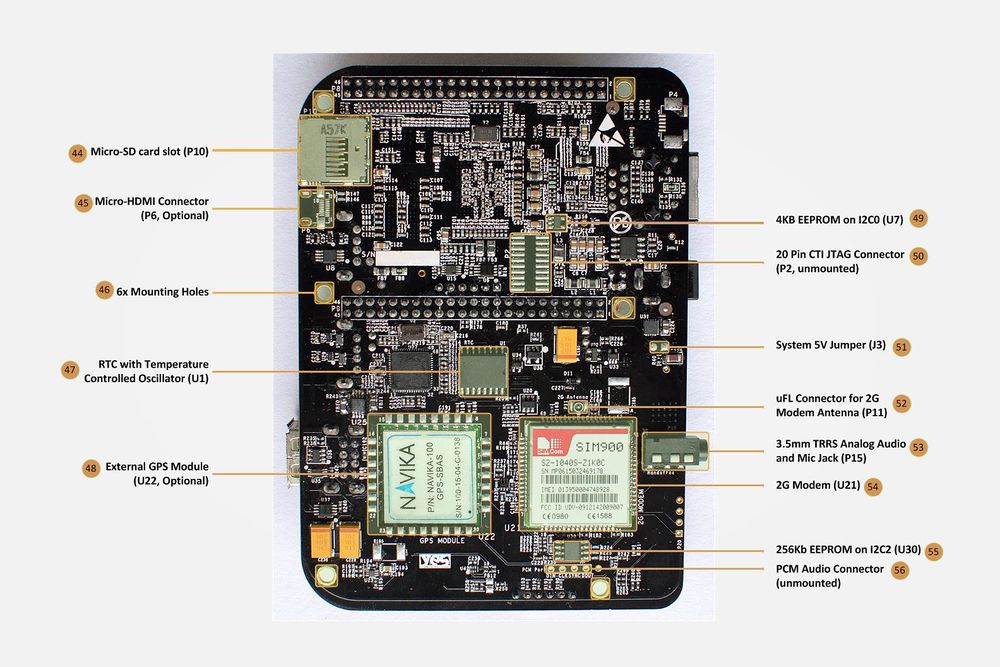
Following images give a proper understanding of the VIBE2 :
Beaglebone Section
- Processor VIBE2 uses TI's Sitara ARM cortex-A8 AM3352 1 GHz processor (AM3352BZCZ100) which is different from 1GHz AM3358 (AM3358BZCZ100) used in original Beaglebone Black. The differences between the two being AM3352 does not have PRU subsystem, EtherCAT and SGX Graphics support.
- USB host ports VIBE2 contains FOUR USB 2.0 HS host ports with type A connector whereas original Beaglebone black has only one. VIBE2 has reconfigured USB0 OTG port as self powered USB hub host ports. So there is no USB client port. USB1 OTG port remains configured as USB 2.0 Host port and used for interface with 3G modem.
- Battery VIBE2 can be powered up by 3.7V Li-ion rechargeable battery with automatic backup switch over circuit from 5V DC input and can power up the whole VIBE2 including 3G/2G modem, all the USB Host ports and HDMI. Original Beaglebone black also supports 3.7V Li-ion Rechargeable battery but with limited functionality of USB host port and HDMI unavailable.
- Ethernet reset VIBE2 includes a standalone ethernet reset circuit over GPIO. This addresses a bug in the original beaglebone black where the Ethernet PHY is not detected at bootup and board had to be reset.
- In VIBE2, the ethernet phy can be individually reset separate from the whole board by toggling gpio GPIO3_21 (GPIO 117).
- To use the GPIO ethernet reset feature, HDMI audio has to be disabled in device tree and then GPIO1_27 (GPIO 59) has to be pulled low so that GPIO3_21 is available for use. Also, HDMI is an optional feature on VIBE2.
- Watchdog Timer VIBE2 includes a watchdog timer circuit which can generate an external reset to PMIC and address the Under Voltage Lockout (UVLO) issue faced in Original Beaglebone Black. If the PMIC TPS65217C enters in UVLO and is not resolved within 10s, watchdog timer will generate an external reset to PMIC.
- Real Time Clock VIBE2 has an accurate Real Time clock with an integrated temperature compensated oscillator and crystal for time keeping operations.
- It includes a 3V non-chargeable coin cell (CR1025/CR1216/CR1220) for standby power.
- RTC (DS3231) is interfaced over I2C2 to AM3352 processor. Its registers can be read to indirectly serve as Temperature sensor too.
- RTC IC generates a 1Hz Square wave signal. This signal is available (optionally) on an uFL connector and GPIO27 when GPS module is not present.
- Extra UART0 header at the edge of the board for easy handling and convenience.
- Fully compatible Beaglebone Black expansion header. Most of the LCD capes are compatible with VIBE2.
For more details on Beaglebone Black refer:[Beaglebone boards]
Radio Section
VIBE has an option between 2G/GPRS modem and 3G/HSPA (3G/CDMA) modem for WAN connectivity.
- 2G modem : The 2G modem is interfaced via UART to UART1 port of the AM3352 processor on VIBE. There are following versions for different regions :
- Quad-Band(2G-Q) : For Global connectivity covering bands GSM 850/EGSM 900/DCS 1800/PCS 1900 with data rates of 85.6kbps DL/42.8kbps UL.
- Dual-Band(2G-D) : For Asia/Europe connectivity covering bands EGSM 900/DCS 1800 with data rates of 85.6kbps DL/42.8kbps UL.
- 3G modem : The 3G modem is interfaced via USB2.0 HS on USB1 Host port of AM3352 processor on VIBE. There are following versions for different regions in both GSM/HSPA and CDMA/EVDO :
- 3G HSPA-A (3GH-A) : For Asia/Europe connectivity covering bands WCDMA 2100 and GSM 850/EGSM 900/DCS 1800/PCS 1900 with data rates of 7.2Mbps DL/5.76Mbps UL.
- 3G HSPA-B (3GH-B) : For Americas connectivity covering bands WCDMA 2100/850 and GSM 850/EGSM 900/DCS 1800/PCS 1900 with data rates of 7.2Mbps DL/5.76Mbps UL.
- 3G HSPA-C (3GH-C) : For Asia/Europe/Australia Connectivity covering bands WCDMA 2100/900 and GSM 850/EGSM 900/DCS 1800/PCS 1900 with data rates of 7.2Mbps DL/5.76Mbps UL.
- 3G HSPA-D (3GH-D) : For Global connectivity covering bands WCDMA 850/1900/2100 and GSM 850/EGSM 900/DCS 1800/PCS 1900 with data rates of 3.6Mbps DL/384kbps UL.
- 3G CDMA (3GC-A) : For Global connectivity covering bands CDMA 800/1900 with data rates of 3.1Mbps DL/1.8Mbps UL.
- 3GH-A/B/C and 3GC-A modems create ports /dev/ttyUSB0, /dev/ttyUSB1 and /dev/ttyUSB2 with ports assigned as :
- a. /dev/ttyUSB0 : Modem port and AT commands port
- b. /dev/ttyUSB2 : AT commands port
- 3GH-D modem creats ports /dev/ttyUSB0, /dev/ttyUSB1, /dev/ttyUSB2, /dev/ttyUSB3 with ports assigned as :
- a. /dev/ttyUSB1 : AT commands port
- b. /dev/ttyUSB3 : Modem port and AT commands port
Both 2G/3G modems have following control interfaces :
- a. Modem Hard reset over GPIO - GPIO44
- b. Modem Hard reset over push button switch - S5
- c. Modem On/Off over GPIO - GPIO45
- d. Modem On/Off over push button switch - S4
- e. Netlight/Signal LED - D15 (this feature is optional in 3GH-A/B/C and 3GC-A modules)
- f. 3G Modem Antenna - On-module GSC connector
- g. 2G Modem Antenna - uFL connector
- h. 3G Modem Wakeup_out/ 2G/3G UART RI - GPIO26
- i. Modem Interface - 2G : UART1 (rx,tx) ; 3G : USB2.0 HS USB1 (and UART1 - optional)
- j. SIM/RUIM card - 6 pin Push-pull mini-sim card connector
- k. Audio - 3.5mm TRRS Analog stereo audio and mic jack(optional)
Additional interfaces for 2G modem only :
- l. UART RTS : I2C1_SCL(UART1_RTS)
- m. UART CTS : I2C1_SDA(UART1_CTS)
- n. UART DTR : GPIO61
- o. UART DCD : GPIO65
- p. 2G Modem Status GPIO : GPIO47
- q. 2G Modem Status LED : D14
- r. 2G Debug UART : on Extra UART0 header
- Default values of GPIO44 and GPIO45 is high.
- USB drivers for the modem (21f5:2012, 21f5:2009, 19d2:ffeb, 19d2:fffe) should be included in the kernel. We provide pre-compiled images with USB drivers included in the kernel.
GPS section
VIBE provides GPS module as an add-on feature to 3G/2G modem and/or as a standalone feature.
GPS module is interfaced on VIBE over UART at UART4 port. NMEA-0183 messages from the GPS modules can be accessed at /dev/ttyO4 port at baud rate of 19200.
Following are the hardware interfaces of GPS module on VIBE :
- Module Interface : UART4(rx,tx) 19200 raw
- Module Reset over GPIO : GPIO46
- Module Reset over push button : S6
- 1 PPS output over GPIO : GPIO27
- 1 PPS output over uFL connector : P14
- GPS Fix Led : D16
- GPS module Power Led (3.3V) : D17
- GPS Antenna : uFL connector P13
- Battery backup for Hot start : 3V coin cell
- GPIO46 should be set to high as Default state for the GPS module to function
- Keep the GPS antenna under open sky for better operations and depending on whether GPS module had a cold, warm or hot start, GPS fix LED will soon start blinking at 1Hz.
Wifi Section
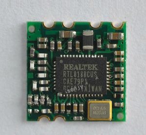
VIBE2 has an add on feature of optional 802.11 b/g/n WiFi wireless. The Wifi module used for this purpose is Realtek RTL8188CUS Module.
The Realtek RTL8188CUS-GR is a highly integrated single-chip QFN-46 pin Wireless LAN (WLAN) USB2.0 network interface controller compatible with the 802.11n specification. It combines a MAC, a 1T1R capable baseband, and RF in a single chip. The RTL8188CUS provides a complete solution for a high throughput performance wireless client.
For more applications follow the document.
Bluetooth Section (BLE)
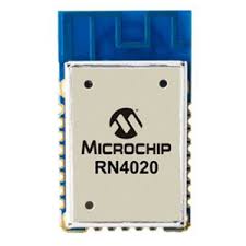
VIBE2 has an add on feature of Optional Bluetooth 4.1 (BLE) wireless. The Bluetooth module used for this purpose is RN4020 microchip.
The RN4020 is a fully-certified, Bluetooth Version 4.1 low energy module for designers who want to easily add low power wireless capability to their products. The small form factor, surface mount module has the complete Bluetooth stack on-board and is controlled via simple ASCII commands over the UART interface. The RN4020 also includes all Bluetooth SIG profiles, as well as MLDP (Microchip Low-energy Data Profile) for custom data. Developers can utilize the scripting feature to enable standalone operation without a host MCU or Processor. The RN4020 can be remote controlled by another module over a secure connection and can be updated via the UART interface or over-the-air.
Following are the control interfaces for BLE:
a. UART2 (/dev/ttyO2) for serial interface
b. deep sleep wakeup (WAKE_SW) - GPIO61
c. dormant state wakeup (WAKE_HW) - GPIO65
d. CMD/MLDP mode - GPIO22
e. Connection LED - D19
f. MLDP event indicator LED - D14 (does not work when 3G modem mounted)
g. Activity indicator LED - D20
NOTE: D20 led glows when module is awake and active. D19 led glows when a connection is being made GPIO61 and GPIO65 should be set to high. GPIO22 is low then module is in CMD mode and in MLDP mode when high.
For more applications follow the document.
Comparison (VIBE and VIBE2)
- Quick Start Guide
- Software Setup Guide
